Surface Characterization Lab
Location: ACMS 110
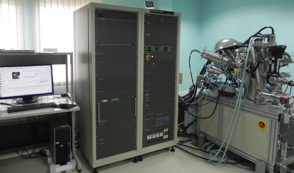
Instrument: X-ray Photoelectron Spectroscopy(XPS) with Auger Electron Spectroscopy(AES) Module
Model/Supplier:PHI 5000 Versa Prob II,FEI Inc.
 |
| The "Surface Characterisation Lab" of ACMS houses a "X-ray Photo-Electron
Spectroscopy (XPS) with Auger Electron Spectroscopy (AES) module and C60 sputter
gun". This facility is available for usage by all the members of the Institute research
community and also, it can be availed for usage for research purposes by Educational
Institutions, National labs/ Private labs and Industries. However, there are certain set
of "Rules and Regulations" laid out to get the best utilisation/ operation/ management
of the facility and also, in the interest safety of machine as well as the operators/users.
It is request that all users co-operate with appreciating the spirit of these "Rules and
Regulation" and kindly comply with. The operation and maintenance of the facility is guided by a "Co-ordination Committee" formally formed by HOD of ACMS and approved by the Institute Authorities. All suggestions and complaints may be registered through any one of the user committee member. The "Usage Charges" is collected towards partial recovery of "cost of maintenance and repairs" and these receipts will be handled as per the Institutes existing norms. Time on the system can be availed by the specified procedures for the same. There are some sample requirements for analysis and certain material will not be accepted for analysis in our facility as mentioned in "Sample Restrictions and Requirement". It is mandatory on all users, both from within Institute and Outside Institute, to submit a declaration on materials being provided to the facility for analysis in the system before availing the facility. Our Instrument and its CapabilitiesXPS with AES Module with Ar ion as well as C60 sputter Guns XPS is a spectroscopic technique to quantitatively measure the elemental compositions
and chemical and electronic states of the elements of a material, including their bond
energy. To obtain the XPS spectra, the sample is irradiated with a beam of X-rays. The
kinetic energy and number of electrons escaping from the top 1 to 7.5 nm of the material
are measured and analyzed. The VersaProbe can be used much like an SEM when
characterizing non-homogeneous materials. |
About Application
XPS is routinely used to analyze a wide variety of materials (both conducting and non-conducting) including inorganic compounds in powder form, metal alloys, semi- conductors, polymers, glasses, ceramics, paints, viscous oils, glues, papers, inks, woods, bones, medical implants and several other biomaterials. The surface characterization of range of materials include metals, polymers, and coatings can be performed through this technique. The unique features of XPS is that it can detect all elements with an atomic number (Z) of 3 (lithium) and above, within 0.01 monolayers of the element on a surface. The ultimate spatial resolution for spectroscopy and mapping is the same, less than 10 μm. The high micro area sensitivity of the VersaProbe makes depth profiling with small diameter x-ray beams very practical.
Access to the Facility
Only "Approved users" and "Approved samples/materials" will be entertained
by facility. The access for usage is through a formal approval from the "Facility
Adminstrators". Institute users will be granted approval to use the facility after
providing valid account numbers with DORD/Institute for charges recovery in the
"Request for Usage Approval". Advance payment is not expected but, it will be
periodically recovered. However, Institute users can deposit advance payments from
which the charges will be deducted and accounts settled.
We encourage researchers from outside IITK use our facility. Efforts will be made to
provide 20-25% Instrument time to outside IITK users. For "Outside IITK Users"
advance payment is expected for getting time slots booked. The charges is to be paid
only as Demand drafts drawn in favour of:
"The Registrar, Indian Institute of Technology, Kanpur".
In the case of direct money transfer, all details of the transfer needs to be provided to the
facility administrator. Acknowledgement of the money received will be provided by the
facility and original receipt from the IITK will be sent as and when received from the
IITK authorities.
Members of Facility Co-ordination Committee
1. Dr. T.G. Gopakumar, Chemistry, (Convener)
(gopan@iitk.ac.in)
2. Prof. Nishith Verma, Chemical Engineering
(nishith@iitk.ac.in)
3. Dr. Sri Sivakumar, Chemical Engineering
(srisiva@iitk.ac.in)
4. Dr. Sarang Ingole, Materials Science and Engineering
(sarang@iitk.ac.in)
CONTACT
| Convener: Dr. T.G. Gopakumar(gopan@iitk.ac.in) | Internal:6830 |
| Lab Incharge: Mr. D.D Pal (ddpal@iitk.ac.in) | Internal:6906 |
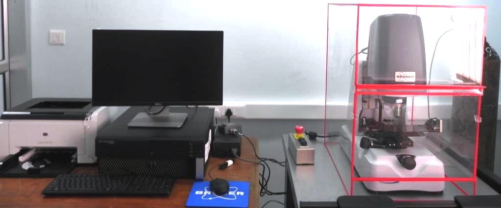
Instrument: Optical Profilometer
Model/Supplier: Bruker Contour GT-K
 |
CONTACT
|