


 |
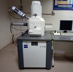
CARL ZEISS EVO 50 Tungsten SEM
Resolution: 2.0 nm @30 kV |
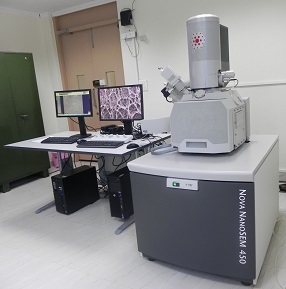 |
FEI NOVA NANO SEM 450 Field Emission SEM
Resolution: 1.0 nm @30 kV
Attachments: EDS & EBSD |
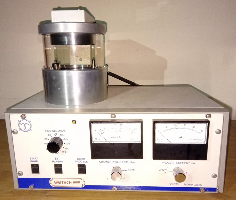 |
EMITECH SC 7620 Sputter coaterMake: EMITECHType: Sputter coating Purpose: Conducting surface Coating Thickness: Few nm Key Features: Compact design Simple operation Glow discharge capability Adjustable height specimen stage Easy change sputter targets - Gold/Palladium (Au/Pd) Recommended Materials: Non conducting materials |