-
Vector Network Analyzer
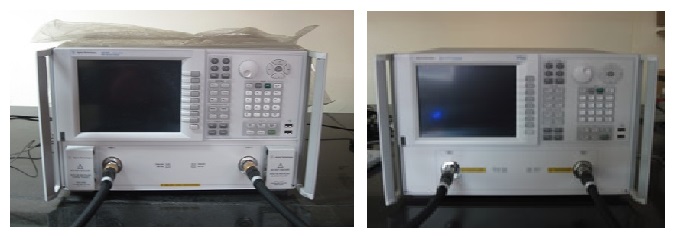
The Network Analyzer is a general purpose device, which can measure both linear and non linear behaviour of devices in the RF and Microwave frequency range. It measures the reflection and transmission coefficients of the device under test (DUT) in the specified frequency range by exciting the DUT with the RF source, and measuring the response. The Network Analyzer consists of two ports, a control panel, an information display and two RF cables to connect the DUT with the analyzer. The types of these cables depend upon the frequency range of operation. One of the important steps in the measurement using Vector Network Analyzer is to do a proper calibration at the measurement reference planes.
We have two network analyzers in the lab.
1. Agilent N5230C PNA-L Microwave Network Analyzer
- 10 MHz to 20 GHz
- 2 ports with two built-in sources
- 110 dB system and 122 dB receiver dynamic range, 32,001 points, 32 channels
- < .006 dB rms (Option 22x)
- Measurement speed: 4 to 9 µs per point
2. Agilent E8361C PNA Microwave Network Analyzer
- 10 MHz to 67 GHz
- 94 dB of dynamic range and <0.006 dB trace noise (specified to 67 GHz, with operation to 70 GHz)
- <26 usec/point measurement speed, 32 channels, 20,001 points
- TRL/LRM calibration, on-wafer, in-fixture, waveguide, and antenna measurements
- Mixer conversion loss, return loss, isolation, and absolute group delay
- Amplifier gain compression, harmonic, IMD, and pulsed-RF
-
Measurement with coaxial line connectors
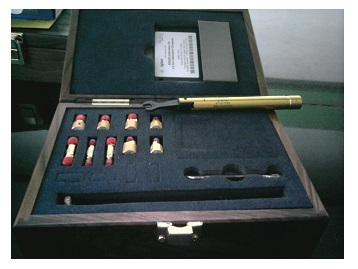
The lab has facility for characterizing any microwave device having coaxial line interface. The approrpiate calibration kit is available to calibrate the Network analyzer in order to facilitate quite accurate measurement of components fitted with the 3.5 mm or similar types of connectors.
The calibration kit includes:
- Offset opens and shorts, and broadband loads.
- Three 3.5 mm adapters.
- 5/16 in.,90 N-cm torque wrench.
-
Measurement of dielectric properties of materials over a wide frequency band
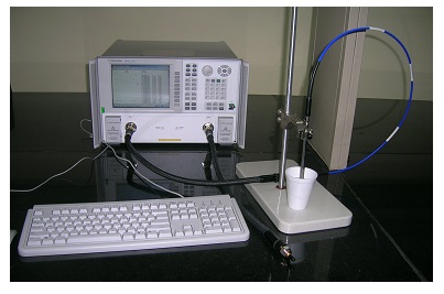
The lab has the facility of measuring dielectric properties of materials over a wide frequency band using the dielectric probe kit. The facility is based on the Dielectric Probe Kit, which comes along with the vector network analyzer and associated microwave components. The established facility enables one to determine the intrinsic electromagnetic properties of wide range of materials in the broad frequency range of 200 MHz to 20 GHz. As the dielectric properties of materials are related with their molecular structure, the measurement of dielectric properties leads to much other useful information. The dielectric probe kit is one of the most useful methods for electromagnetic characterization of materials in the broad frequency range. The complete system is based on a network analyzer, which measures the material‘s response to the RF or microwave energy. The probe transmits a signal into the material under test (MUT), and the reflected data is used to determine the dielectric properties of the MUT using special software, which is supplied along with the kit. The probe supplied with the kit is quite versatile, and dielectric measurements can be carried out by simply immersing the probe into test liquids or semi-solids without requiring any special fixtures or containers. The procedure does not require any sample preparation, and the measurements are quite often non-destructive and can be made in real time. The software controls the network analyzer and guides the user through easy setup and measurement procedures. The complex permittivity of the test sample is finally displayed on screen of the network analyzer using the supplied software. The limitation of this equipment is that it does not provide very accurate measurements of sloids because of the problem of the possible air gap between the probe and the material under test.
The major components of the dielectric probe kit are as follows :
- Performance Probe
- Probe Stand
- 20 GHz PNA Series network analyzer
- Dielectric Probe Software
Dielectric Probe Kit
The dielectric measurement facility in the microwave frequency band was established in the Department of Electrical Engineering in the year 2010 with CARE grants from IIT Kanpur. The facility is based on the Agilent Technologies 85070E Dielectric Probe Kit, which comes along with the vector network analyzer and associated microwave components. The established facility enables one to determine the intrinsic electromagnetic properties of wide range of materials in the broad frequency range of 200 MHz to 20 GHz. As the dielectric properties of materials are related with their molecular structure, the measurement of dielectric properties leads to much other useful information which is otherwise quite difficult to obtain. These properties are usually expressed in terms of permittivity and permeability, which might change with frequency, temperature, orientation, mixture, pressure etc.
-
Waveguide measurements
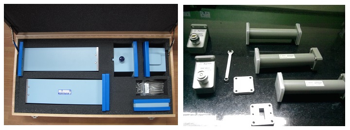
The lab has a number of rectangular waveguide calibration kits operating in various frequency bands for characterizing any device having the waveguide interface. These kits are configured for use in performing full two port:
1. TRL
- Thru
- Reflect
- Line
2. OSLT
- Short
- Open
- Broadband Load
- Thru
The TRL and OSLT calibrations are the two standard methods for performing error corrections. This lab is equipped with expertise of measuring dielectric properties of materials in the microwave frequency range using the rectangular waveguide approach.
Waveguide Calibration Kit
The Agilent X11644A calibration kit contains the precision mechanical standards required to calibrate the systematic errors of Agilent network analyzers. This calibration kit has a precision airline for performing the Thru-Reflect-Line (TRL) calibration, the most accurate error-correction technique for coaxial measurements. This kit also contains a flush short circuit, a precision shim, and a fixed termination.
-
Material testing

The measurement of dielectric properties of materials forms the basis of microwave testing of objects and media in order to determine their inner structure using microwaves. The reflection and transmission coefficients of the material-under-test (MUT) are measured with the help of a vector network analyzer by placing the MUT either between the pair of antennas or into a section of rectangular waveguide. The reconstruction of the dielectric properties is obtained in terms of the measured scattering data using the in-house developed algorithm.
References:
-
Microwave imaging and non-destructive testing
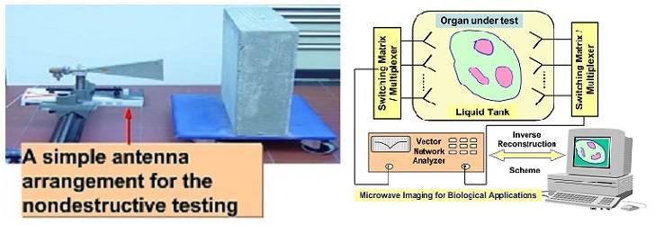
The lab has facility of getting the sub surface image of the test object using the microwave technique. The overall procedure requires the measurement of reflection and transmission coefficients of the object under test in the specified frequency range using an appropriate experimental setup. The dielectric image of the test object is then obtained in terms of measured scattering data using the inverse reconstruction algorithm. The Microwave Non-Destructive Testing is used for applications such as detecting the quality of walls and buildings, finding the quality of concrete strucrtures in Civil Engineering areas etc. The microwave imaging technique has various applications in the field of biomedical and industrial field.
-
RF & microwave filter design
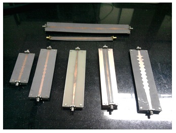
The planar microwave filters have gained much popularity in recent years for various RF and microwave applications because of their advantages such as light weight, low cost, easy integration with active devices etc. The advantage of using the electromagnetic inverse scattering procedure for the RF and microwave filter design is that one can directly obtain the physical layout of planar filter in terms of the specified filter characteristics. The electromagnetic inverse scattering procedure is a method, which can quite conveniently be used to design microwave planar filters of continously varying impedance profile. The required impedance profile can then be converted into dimensions of the appropriate filter for achieving the specified frequency response.
-
Digital Oscilloscope(4 GHz, 20GSa/s)
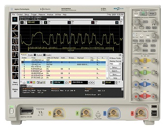
The lab is equipped with a 4 channel, 4Ghz bandwidth, 20GSa/s oscilloscope. The oscilloscope can be used with keyboard and mouse interfaces through USB. The software platform is based on windows 7 allowing easier access to saved data and other graphical contents.
The main features of the oscilloscope are:
- 4 GHz bandwidth across all 4 analog channels
- 20 GSa/s max. sample rate
- Standard 20 Mpts memory per channel, upgradeable to 1 Gpts.
- Advanced triggering coupled with superior specifications give you precise signal representation
- Logic Analyzer: Add 16 integrated, deep-memory digital channels to see critical data values and timing relationships