Major Facilitiess
Explore multiple facilities under one roof focuses on the development of biosensing technologies for various applications, primarily targeting health diagnostics and environmental monitoring
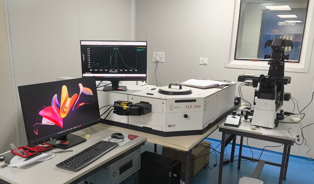
Edinburgh Instruments FLS1000 Spectrofluorimeter (TRPL Facility)
The Edinburgh Instruments FLS1000 Spectrofluorimeter, recently commissioned at the Centre for Nanosciences, IIT Kanpur, is a high-performance, modular fluorescence spectroscopy platform designed for comprehensive steady-state and time-resolved photoluminescence characterization of fluorescent materials. The instrument supports a wide range of applications across nanoscience, materials science, chemical sciences, and biological research, with particular relevance to optoelectronic materials, quantum dots, upconversion nanomaterials, biosensing probes, powders, thin films, and crystalline solids.
Equipped with multiple excitation sources spanning continuous-wave, microsecond, nanosecond, and picosecond time regimes, the FLS1000 enables detailed investigation of emission and excitation spectra, fluorescence lifetimes, excited-state dynamics, energy transfer processes, and quantum efficiency parameters. Its modular architecture allows seamless switching between steady-state spectroscopy, lifetime measurements over several orders of magnitude, and advanced time-resolved techniques such as time-resolved photoluminescence (TRPL) and time-resolved emission spectroscopy (TRES).
The availability of specialized accessories, including an integrating sphere for absolute quantum yield measurements and an integrated fluorescence microscope for spatially resolved steady-state and time-resolved studies, makes this system particularly powerful for correlating optical properties with morphology and spatial heterogeneity. This combination positions the FLS1000 as a state-of-the-art fluorescence characterization facility suitable for both fundamental research and application-oriented studies.
Excitation Sources and Measurement Regimes
1. Xenon Continuous-Wave Lamp
- Wavelength range: ~250–1000 nm
- Emission, excitation, 3D EEM mapping
- Synchronous fluorescence spectroscopy
- Applications: dyes, nanomaterials, biomolecules, optoelectronics
2. μF² Xenon Flash Lamp
- Wavelength range: ~250–1000 nm
- Time regime: Microsecond–millisecond
- Technique: Multi-Channel Scaling (MCS)
- Applications: phosphors, triplet dynamics, OLED materials
3. Picosecond Pulsed Diode Lasers (EPL)
- 375, 405, 450, 485 nm
- Technique: TCSPC
- TRPL & TRES (ps–ns)
- Quantum dots, nanocrystals, biosensing probes
- No mapping in pulsed mode
4. Upconversion Excitation Source
- Excitation wavelength: 900 nm
- UCNPs and NIR-excited visible emitters
- Bioimaging and photon-conversion materials
Advanced Measurement Accessories
Integrating Sphere
- Absolute photoluminescence quantum yield (PLQY)
- Quantum efficiency–related parameters
- Powders, thin films, and solutions
- OLED materials, phosphors, fluorescent nanomaterials
Integrated Fluorescence Microscope
- Spatial fluorescence mapping
- Time-resolved fluorescence imaging
- TRPL and TRES with spatial resolution
- Rare and advanced facility in India
Sample Handling & Measurement Limitations
- Powder, thin film, liquid, and bulk crystalline samples
- Solid sample holders for routine photoluminescence measurements
- Detector: Red-sensitive PMT-900 (cooled)
- Detection range: ~200–870 nm
- Emission beyond 870 nm not detectable
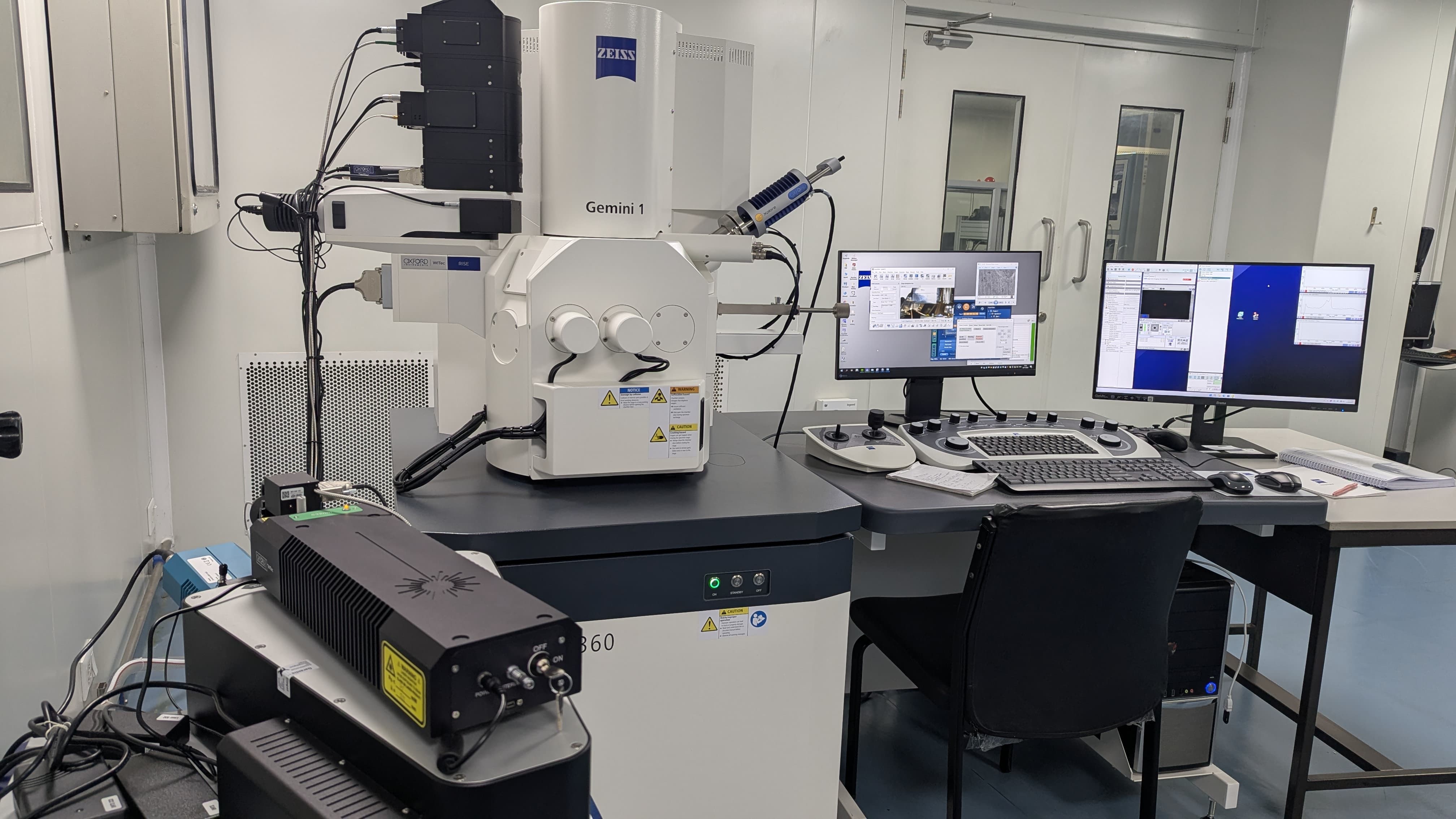
FESEM Integrated with Micro Raman and EDS
The FESEM integrated with Micro Raman and Energy Dispersive X-ray Spectroscopy (EDS) is a powerful correlative characterization facility that enables simultaneous high-resolution surface imaging, elemental composition analysis, and molecular vibrational fingerprinting. This integrated system is designed to provide complementary structural, chemical, and spectroscopic information from the same region of interest, making it particularly valuable for advanced materials and nanoscience research.
By combining electron microscopy with Raman spectroscopy and EDS, users can correlate morphology with chemical composition and molecular structure, enabling deeper insight into heterogeneous, multi-component, and functional materials. Below are the core capabilities and technical specifications mentioned.
Core Capabilities
- High-resolution surface and microstructural imaging
- Elemental analysis and compositional mapping using EDS
- Molecular and phase identification using Micro Raman spectroscopy
- Correlative analysis from the same sample location
- Non-destructive Raman measurements on sensitive samples
Typical Applications
- Nanomaterials and nanocomposites
- Thin films and coatings
- Semiconductors and electronic materials
- 2D materials, carbon materials, and oxides
- Failure analysis and contamination studies
Sample Handling Capabilities
- Solid bulk samples and pellets
- Thin films on various substrates
- Powders and particulate samples
- Micro- and nano-structured materials
- Conductive and non-conductive samples (with appropriate preparation)
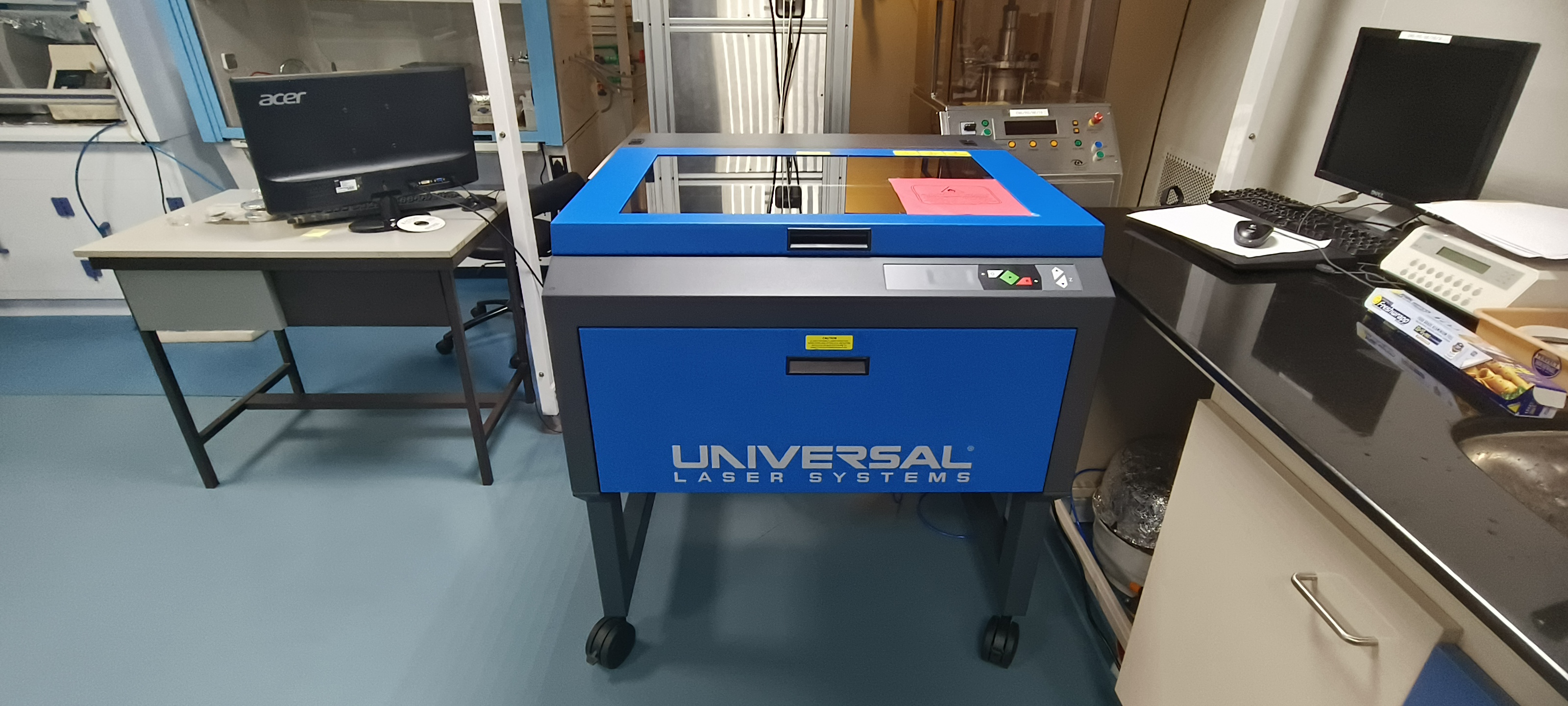
Laser Engraver
The Laser Engraver is a precision laser-based system used for engraving, cutting, and micro-patterning of a wide range of materials such as polymers, acrylics, wood, leather, masking films, select foams, and compatible soft metals. The system offers high accuracy, controlled depth, and reliable performance at micro-scale resolution for research, prototyping, and fabrication needs.
Equipped with a high-power CO₂ laser source and advanced optics, the engraver enables both fine-detail engraving and practical material cutting with excellent repeatability. The motorised Z-axis allows processing of substrates with varying thicknesses and weights, making the system suitable for diverse sample geometries and experimental requirements.
This facility is particularly useful for rapid prototyping, micro-pattern fabrication, device marking, mask preparation, and customized sample processing for research and development activities in materials science, nanotechnology, and biosensing applications.
Technical Specifications
- Laser Type: CO₂ Laser
- Laser Power: 50 W
- Wavelength: 10.6 µm
- Processing Envelope: 24" × 18" × 8.5" (610 × 457 × 216 mm)
- Optics: 2.0” HPDFO lens
- Z-Axis: Motorised Z-axis supporting substrates up to 40 lbs (18 kg)
Core Capabilities & Performance
- Cutting, engraving, and marking of a wide range of materials using a 50 W CO₂ laser (10.6 µm).
- 2.0” HPDFO lens enables high resolution, precise energy density control, and limited direct metal marking with CO₂ lasers.
- Best suited for deeper engraving and substantial cutting on acrylic, wood, leather, and compatible soft metals.
- Typical materials include thicker acrylic, plywood, masking films, leather, and select foams.
- Cutting performance improves significantly while maintaining fine engraving detail.
- Higher power increases processing speed and throughput; adequate ventilation is recommended.
- Integrated optics protection with gas assist improves lens cleanliness and extends optic lifetime.