Welcome to the Chip Gallery, a showcase of cutting-edge research and innovation from our laboratory. This collection presents fully taped-out Integrated Circuits (ICs), which represent the tangible success of translating complex theoretical designs into functional hardware. The chips displayed here mark significant milestones in RF, mixed-signal, and sensor interface technology.
This is just the beginning!
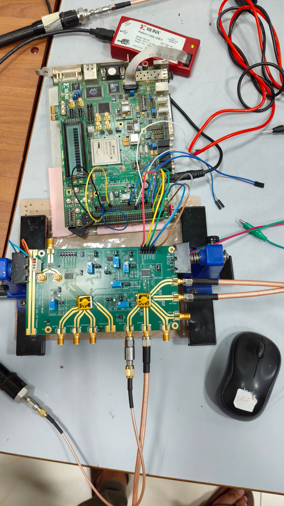
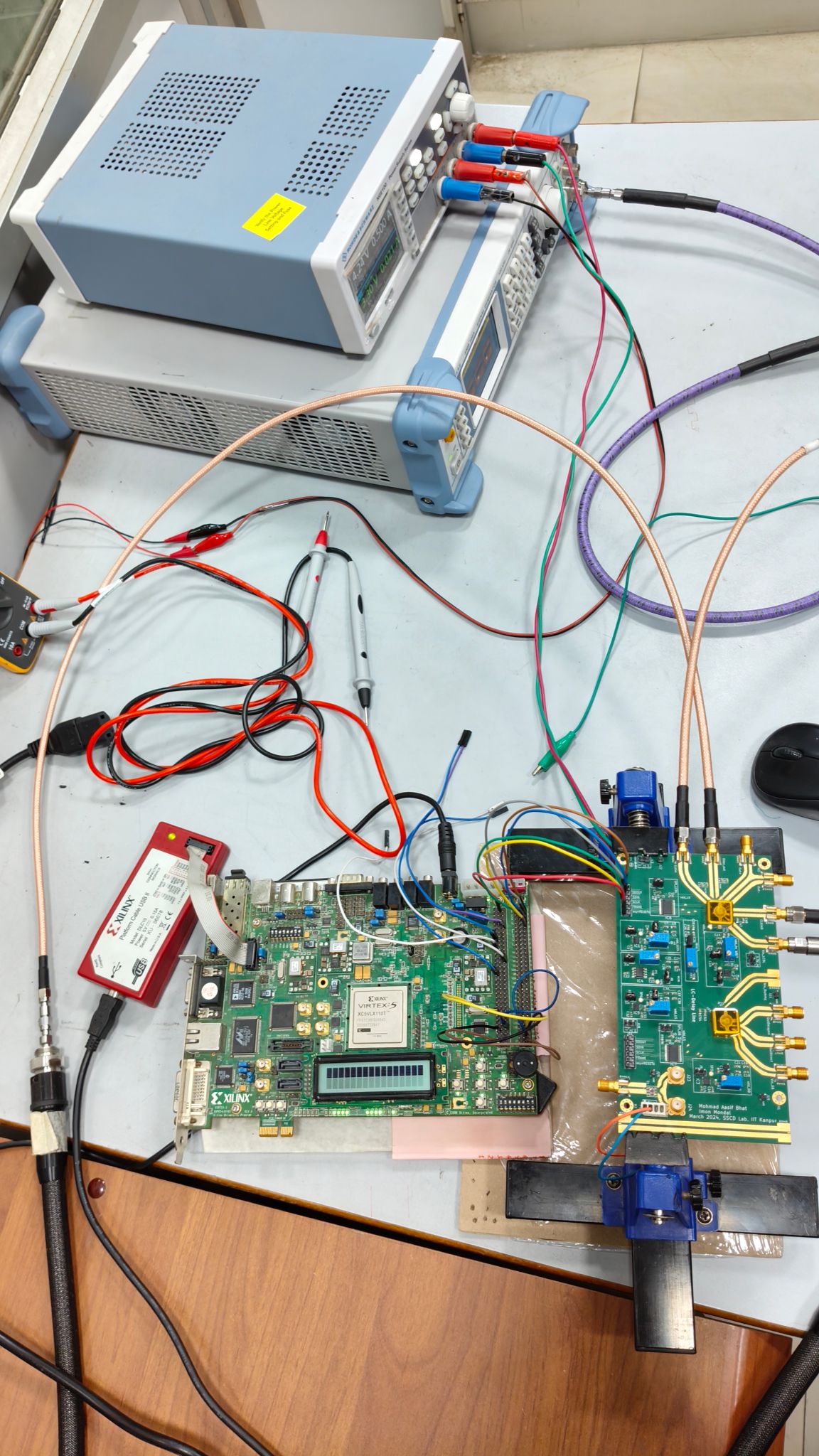
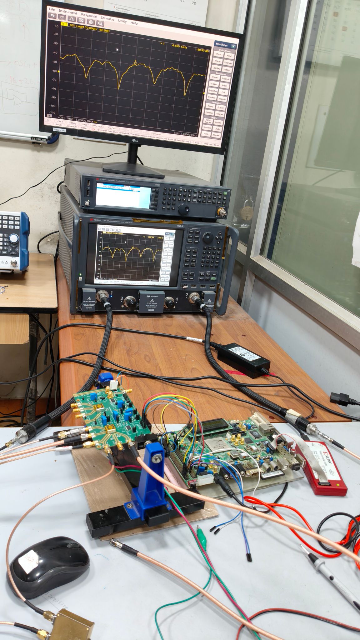
A compact (0.35 mm²), power efficient (16 mW), all-passive LPTV switched-LC delay-line with a tunable true-time-delay range of 0.2–1.1 ns over 3–5.5 GHz RF in 65 nm CMOS.
[ Mohmad Aasif Bhat and Imon Mondal, IEEE JSSC 2025]
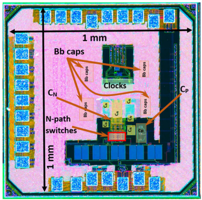
An all-passive source-parasitic insensitive N-path filter, achieving sub-3dB noise figure and +21dBm OOB IIP3 over 0.5-1GHZ RF with complex impedance matching in 65nm CMOS.
[Sameer Kumar and Imon Mondal, IEEE JSSC 2025]
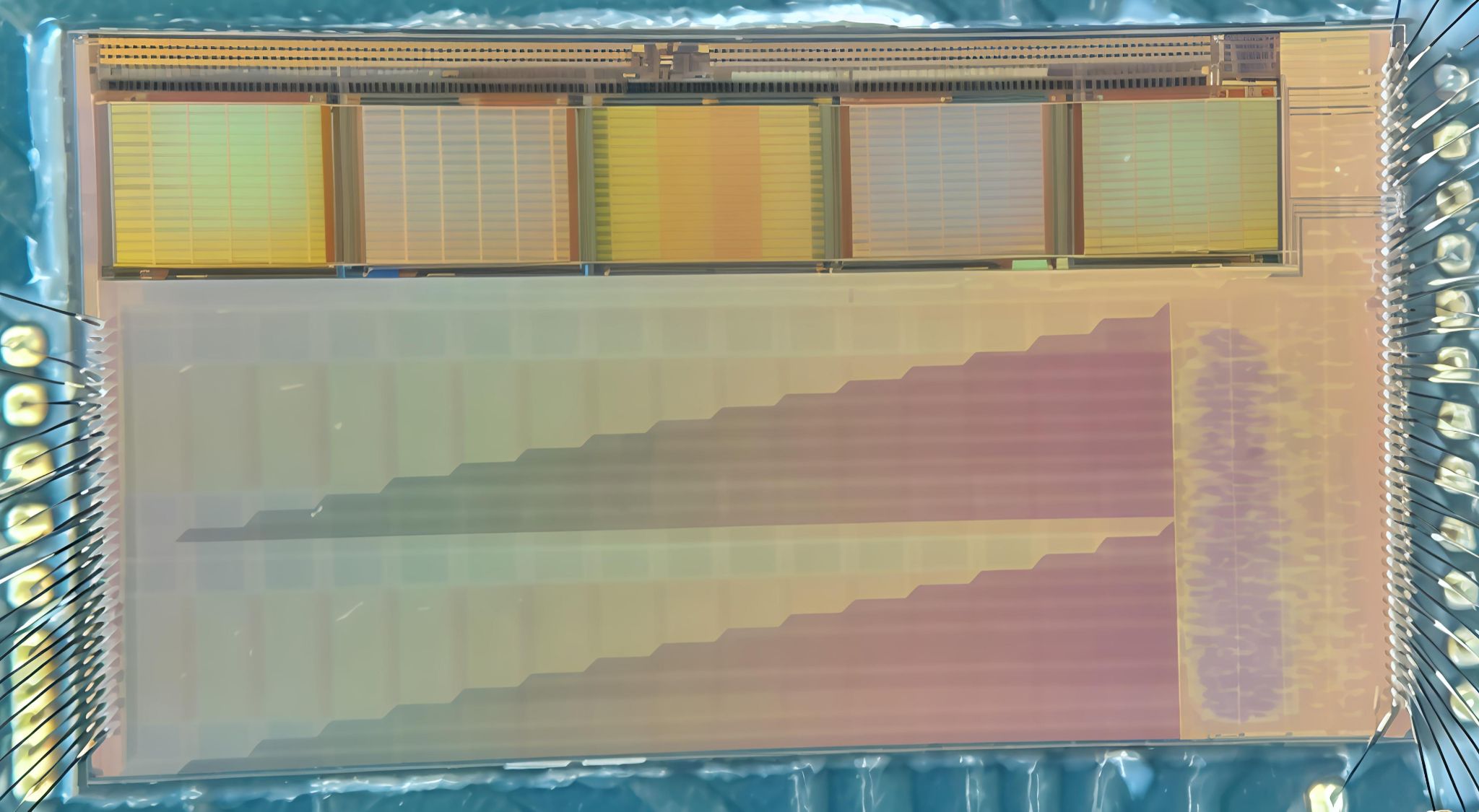
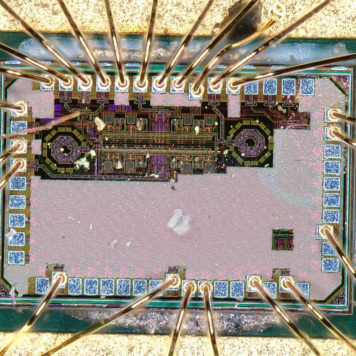
A 7mm X 4mm Readout Integrated Circuit (ROIC) designed for a 640×480 infrared focal-plane array (FPA), featuring multi-channel readout, segmented architecture, and synchronized timing in 130nm CMOS. It incorporates a two-stage calibration with off-chip SRAM and on-chip offset correction for enhanced accuracy.
[ Abhishek Kumar and Imon Mondal]
Some snaps of the PCBs and setups used to test our designed ICs: